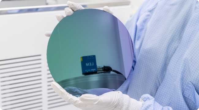
Deposition processes are used throughout the semiconductor manufacturing process to create integrated circuits (ICs). Nearly every step in the device fabrication process uses a form of thin-film deposition. Thin films are used in passive roles as hard masks, antireflection coatings, passivation layers, and encapsulation, as well as in active device roles such as capacitors, inductors, contacts, and interconnects. Thin-film materials include dielectrics, metals, and polymers. Many of them involve a plasma deposition process to deliver the desired film properties within a defined thermal budget. At Plasma-Therm®, we’ve fine-tuned an assortment of plasma-enhanced deposition processes to help you achieve precisely the film features you need for optimal device performance.
From dielectric films to metallization, dopants to anti-reflectant coatings and encapsulation, plasma-based deposition processes deliver on performance, precision, flexibility, and process control.
PECVD
Plasma-enhanced chemical vapor deposition (PECVD) lets you maintain relatively low wafer temperature while achieving and controlling desired film properties such as stoichiometry, refractive index, stress, and step coverage, and also maintaining highly uniform film deposition.
HDPCVD
High-density plasma chemical vapor deposition (HDPCVD) is a special form of PECVD that uses an inductively coupled plasma (ICP) source to give you a higher plasma density than a standard parallel-plate PECVD system. For this reason, high-quality films are produced at even lower temperatures than with conventional PECVD.
F.A.S.T.®
Fast atomic sequential technology (F.A.S.T.) stands at the crossroads of chemical vapor deposition (CVD) and atomic layer deposition (ALD). The technology is a derivative of ALD, benefiting from the flexibility of a dual-channel showerhead and pulsed gas injection with adjustable in situ plasma pulsing. The result is films that take advantage of ALD-like conformality but at significantly higher deposition rates.
IBD
Ion beam deposition (IBD) is used to deposit thin films from a wide range of materials for various production processes. Tilt, substrate rotation, and ion-beam assist features provide capabilities not found in other deposition technologies.
PVD
Physical vapor deposition (PVD) with sputtering technology allows for deposition processes of a wide range of metals for front- and backside applications and reactive sputtering of materials such as AlN, ScAlN, and AlOx.
Explore all Deposition Products
Find all our deposition products, processes, capabilities, and brands here.
CONTACT A SALES SPECIALIST
Deposition Product by Process Capabilities
Not sure which of our deposition process tools is right for your applications? Use this table as your guide.
| * indicates products with Add-on options | PECVD | HDPCVD | F.A.S.T.® | IBD | PVD |
|---|---|---|---|---|---|
| * VERSALINE® | PECVD | HDPCVD | IBD | ||
| QuaZar™ | IBD | ||||
| Eclipse™ | PVD | ||||
| Endeavor™ | PVD | ||||
| KOBUS™ | F.A.S.T.® |
NEED ASSISTANCE?
Let our experts help you customize our processes solutions for your applications.