While some semiconductor manufacturers continue to pursue Moore’s Law with device scaling, others are focused on advanced packaging technology to deliver on power, performance, area, and cost (PPAC). With chiplets, heterogenous packaging, wafer-level packaging designs, and more, the bar for better PPAC is being raised.
From deep silicon etch (DSE™) and our award-winning Fast Atomic Sequential Technology (F.A.S.T.®) to our proprietary high-density radical flux (HDRF™) process technology and revolutionary plasma dicing capabilities, we are helping lead semiconductor and advanced packaging innovation. Whether it be plasma dicing on tape (PDOT™), plasma dicing on carrier (PDOC), or plasma dicing before grind (PDBG), we have it covered.
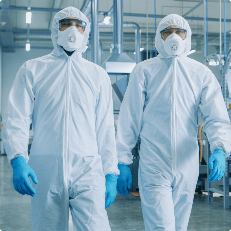
Whether you are an integrated device manufacture (IDM), pure-play foundry, or outsourced semiconductor assembly and test service (OSAT) provider, our systems and solutions, along with our knowledge of process nuances and subtleties, will help you remove risk, increase efficiency, enhance capacity, and expand your yield.
Etch
For high-aspect-ratio through-silicon vias (TSVs) and backside thinning processes, plasma etch is the key to high-yielding devices. Our DSE gives you smooth surfaces and etch depths of >100µm.
Deposition
High-volume, low-cost TSVs are now attainable using our fast atomic sequential technology (F.A.S.T.®) deposition processes that approach atomic layer deposition (ALD) performance levels at a speed approaching chemical vapor deposition.
Material Modification
Our HDRF low-temperature technology is proven for photoresist, polymer residue removal, and bond pad cleaning. These surface preparation steps are critical to the reliability of your high-density fan-out wafer level packaging (FOWLP), chiplet, and 3D IC devices.
Plasma Dicing
Plasma-etch dicing processes are ideal for ultra-thin die for 3D stacking. By replacing traditional blade dicing with plasma etch, you’ll eliminate chipping and cracking and improve your throughput and yield.
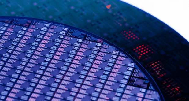
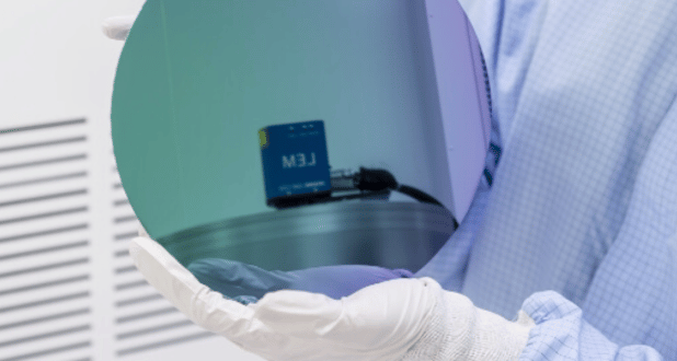
Semiconductor and Advanced Packaging Applications
EXPLORE ALL PROCESS TECHNOLOGY
We continuously improve our plasma etch, deposition, and dicing technology to help you build the best products on the market.
NEED ASSISTANCE?
Let our experts help you customize our processes solutions for your applications.