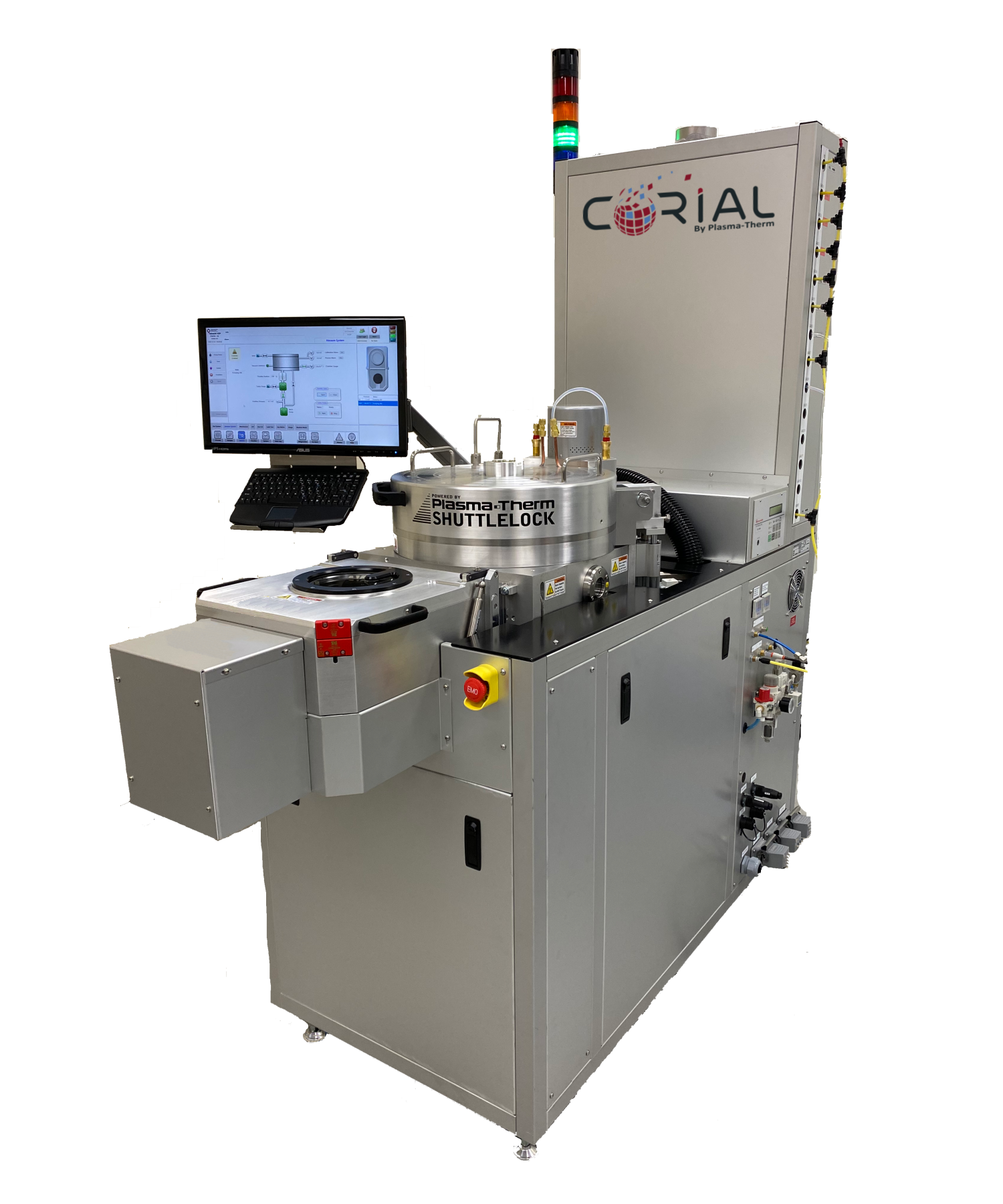
At the sub-10 nm scale, conventional etch processes can’t deliver the level of control you need. Atomic-level precision manufacturing ensures ultra-high etch selectivity, decreased damage and control at the nanometer scale.
ALE technology lets you control material removal from a substrate, layer-by-layer, where the etch thickness is on the order of magnitude of a monolayer. The process recipe parameters and reactants used in our ALE systems deliver etching with exceptional precision and selectivity to masks layers. When you need to move layer by layer, our ALE systems get it done.
Great Alternative
This technology has long been of growing interest for academic and industrial applications as an alternative to continuous etching, and as an essential counterpart to atomic-layer deposition.
Widely Accepted
Despite its apparent simplicity, it took several decades since the discovery of the ALE mechanism for the technology to gain broad acceptance and applicability.
Self-Limited
Self-limited reaction is a key characteristic of atomic scale etching. Ideally with ALE, adsorption and desorption steps are self-limited at a maximum rate equivalent to 1 monolayer (ML) per cycle.
Materials
The materials suitable for ALE range from semiconductor and dielectric materials (Si, III-V, SiO2, Si3N4) to metals and 2D materials such as graphene, MoS2 etc.
OUR ALE PRODUCTS
EXPLORE TECHNICAL PAPERS
Want to learn more about this topic? Click here to review technical papers on ALE principles, practices and outcomes.
SEE ALL ETCH PRODUCTS
To review all our etch products, processes, capabilities, and brands, click here.
NEED ASSISTANCE?
Let our experts help you customize our processes solutions for your applications.
