FAQ
You have questions, we have answers!
As the authorities on plasma process equipment, we’re asked to address different pain points. From how we work to service offerings and tool adjustments, we tasked our knowledgeable team with answering the most frequently asked questions here. If you don’t see yours, drop us a note and one of our dedicated team members will contact you.
WHITEPAPERS AND TECHNICAL PAPERS
A New Production Solution for High Selective and Low-Damage Etching of GaAs-Based Devices
Conventional reactive ion etching (RIE) has generally been used for selective etching of GaAs over…
The Effects of Increasing the Aspect Ratio of GaAs Backside Vias
To support the current trend in industry of working towards higher via densities which could…
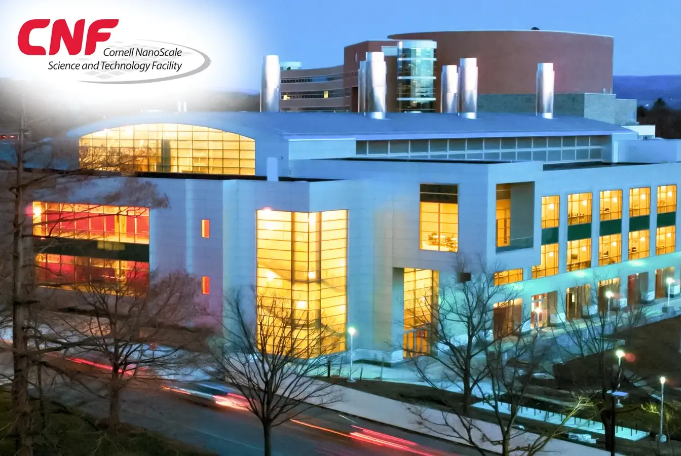
Assessing Deep Reactive Ion Etch (DRIE) at CNF
Cornell University’s Nanoscale Science and Technology Facility (CNF) recently took delivery of a VERSALINE® deep silicon…
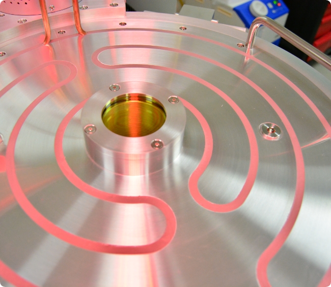
Optimization of Low Stress PECVD Silicon Nitride for GaAs Manufacturing
Unaxis solutions for plasma-enhanced chemical vapor deposition (PECVD) silicon nitride (SiNx) are used extensively in…
NEED ASSISTANCE?
Let our experts help you customize our processes solutions for your applications.