Archives: Applications

Wireless Connectivity

5 g tower with sunset

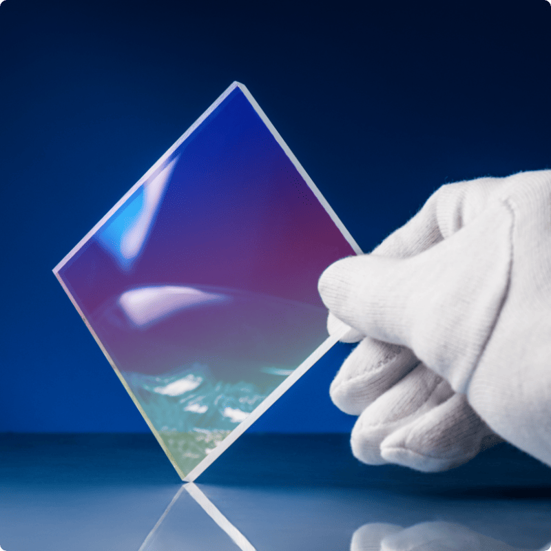
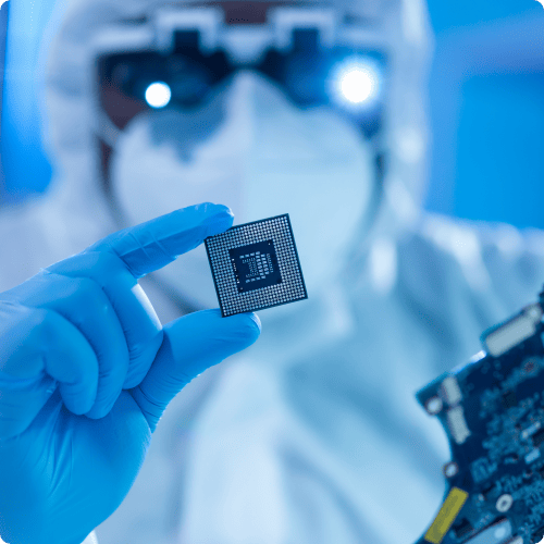
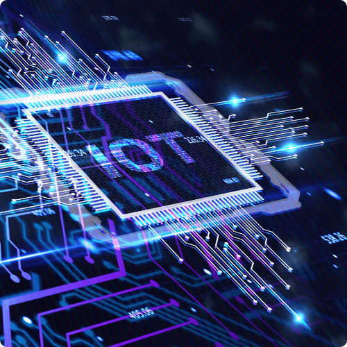
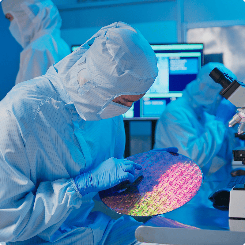
The ongoing push for global connectivity that relies on mobility, the Internet of Things (IoT), and 5G calls for robust, leading-edge wireless technology. The devices underpinning wireless technology are built using compound semiconductor materials.

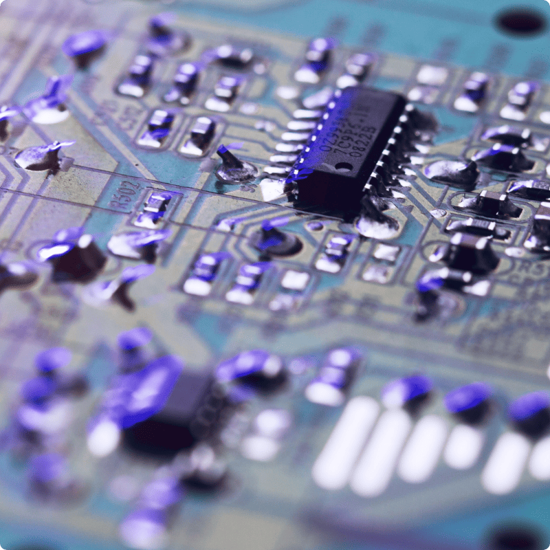
Compound semiconductor devices include heterojunction bipolar transistors (HBT), high-electron-mobility transistors (HEMTs), and surface acoustic wave (SAW) and bulk acoustic wave (BAW) technology used in digital, analog, and mixed integrated circuits for radio, power, and other high-frequency applications.

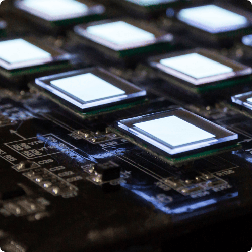
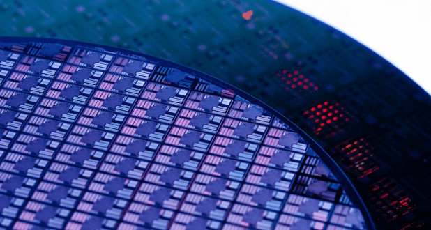
At Plasma-Therm®, we support compound semiconductor device manufacturing with our etch, deposition, ion beam, and plasma dicing tools.

Etch 

If you’re looking for reproducibility and a process library for the wide range of materials used in wireless applications, then Plasma-Therm has you covered. VERSALINE® systems provide the range of inductively coupled plasma (ICP) and ion beam etch (IBE) needed for compound semiconductor, metals, dieletrics, and piezoelectric materials used in SAW, BAW, and film bulk acoustic resonator (FBAR) filters. 

Deposition

Just one example of our innovative approaches is our advanced plasma-enhanced chemical vapor deposition (PECVD) helium dilution technology, which provides a stress-free silicon nitride deposition process to prevent device damage. 

Thermal Processing

Our industry-standard thermal processing technology works on substrates up to 200mm in diameter. Fast wafer size changes accommodate the range of substrates being used. 

Plasma Dicing

Our Singulator® system is ideal for damage-sensitive compound semiconductors like gallium arsenide (GaAs) and indium gallium arsenide (InGaAs). You get smooth sidewalls, improved die strength, street sizes <10µm, and any shape die you want. 

Wireless & Connectivity Applications

The world is becoming more connected every day. Wireless mobility that relies on 5G and Internet of Things (IoT) devices is pervasive and critical to our goal of enhancing the human experience. In a wireless world, power amplifiers and switches become critical components for communicating between the ever-increasing number of mobile and smart devices.

5G standards require more RF filters in mobile products and network infrastructures than previous generations. They must support higher frequencies and increased bandwidth. Surface acoustic wave (SAW), film bulk acoustic resonator (FBAR), and bulk acoustic wave (BAW) filters are the advanced high-frequency acoustic sensors that are critical to reducing power consumption, improving battery life, and handling the increasing number of RF communication bands.

wireless home

5g tower

radio tower

Explore All Process Technology

We continuously improve our plasma etch, deposition, and plasma dicing technology to help you build the best products on the market.

EXPLORE ALL PRODUCTS

Our easy-to-use plasma-based systems keep pace with your needs and are engineered to provide outstanding performance time after time.

NEED ASSISTANCE?

Let our experts help you customize our processes solutions for your applications.

Photonics

Photonics place purple color

Photonic devices are designed to emit, reflect, transmit, or absorb photons spanning the electromagnetic spectrum from x-rays to the far infrared and have features ranging in size from nanoscale to tens of microns. All this is possible with materials as diverse as indium phosphide (InP), gallium nitride (GaN), silicon-based dielectrics, metals such as gold and platinum, and lithium niobate (LiNbO3). There isn’t any part of life that doesn’t use or rely on photonic devices. Whether for illumination, optotelecommunication, sensing, or displays, photonics is playing the critical role.

Most photonics devices are built using compound semiconductor materials, an area of manufacturing for which Plasma-Therm® is well known. When you partner with us, you’ll be tapping into the expertise that comes from installing more than 1,300 systems in both R&D and production.

Etch

Whether your photonics devices need high temperature for InP etching or ion-beam etching for lithium niobate or low-damage etching for microLEDs, we have it. 

Deposition

You’ll find the right film among our many deposition technologies. With PECVD, HDPCVD, PVD, IBD, RIBD, and F.A.S.T.®, one will provide the film properties you are looking for. 

Wafer Clean

Our high-density radical flux (HDRF™) low-temperature, downstream technology is proven for photonics applications, including photoresist removal without ion exposure, for optimum-quality devices. 

Plasma Dicing

Plasma dicing with the Singulator® system is ideal for damage-sensitive photonics devices. You get smooth sidewalls, improved die strength, street sizes <10µm, and any shape die you want. 

Photonics Applications

Augmented reality and virtual reality (AR/VR) headsets and a variety of displays with devices such as microLEDs, waveguides, and lasers provide users with a full 3D experience and are making human interaction in the metaverse possible.

Powering the Information Age are solid-state lasers, waveguides, and detectors that make up transceivers and operate in conjunction with fiber optics.  

Light is the choice for applications as diverse as biosensors for virus detection or LIDAR for detecting and imaging a deer in the road. 

woman playing with vr

VCSELs and Optoelectronics Tile

micro leds

Explore All Process Technology

We continuously improve our plasma etch, deposition, and dicing technology to help you build the best products on the market.

EXPLORE ALL PRODUCTS

Our easy-to-use plasma-based systems keep pace with your needs and are engineered to provide outstanding performance time after time.

NEED ASSISTANCE?

Let our experts help you customize our processes solutions for your applications.

Advanced Packaging

scientists waling in a lab

While some semiconductor manufacturers continue to pursue Moore’s Law with device scaling, others are focused on advanced packaging technology to deliver on power, performance, area, and cost (PPAC). With chiplets, heterogenous packaging, wafer-level packaging designs, and more, the bar for better PPAC is being raised. 

From deep silicon etch (DSE™) and our award-winning Fast Atomic Sequential Technology (F.A.S.T.®) to our proprietary high-density radical flux (HDRF™) process technology and revolutionary plasma dicing capabilities, we are helping lead semiconductor and advanced packaging innovation. Whether it be plasma dicing on tape (PDOT™), plasma dicing on carrier (PDOC), or plasma dicing before grind (PDBG), we have it covered. 

Whether you are an integrated device manufacture (IDM), pure-play foundry, or outsourced semiconductor assembly and test service (OSAT) provider, our systems and solutions, along with our knowledge of process nuances and subtleties, will help you remove risk, increase efficiency, enhance capacity, and expand your yield.

Etch

For high-aspect-ratio through-silicon vias (TSVs) and backside thinning processes, plasma etch is the key to high-yielding devices. Our DSE gives you smooth surfaces and etch depths of >100µm.

Deposition

High-volume, low-cost TSVs are now attainable using our fast atomic sequential technology (F.A.S.T.®) deposition processes that approach atomic layer deposition (ALD) performance levels at a speed approaching chemical vapor deposition. 

Material Modification

Our HDRF low-temperature technology is proven for photoresist, polymer residue removal, and bond pad cleaning. These surface preparation steps are critical to the reliability of your high-density fan-out wafer level packaging (FOWLP), chiplet, and 3D IC devices. 

Plasma Dicing

Plasma-etch dicing processes are ideal for ultra-thin die for 3D stacking. By replacing traditional blade dicing with plasma etch, you’ll eliminate chipping and cracking and improve your throughput and yield. 

Semiconductor and Advanced Packaging Applications

Applications like artificial intelligence (AI) and high-performance computing to support the deluge of data processing and storage have increased the design complexity of leading-edge logic and memory chips.

Improving semiconductor PPAC calls for high-density advanced packaging architectures like high-density FOWLP, 2.5D interposers, chiplets, and 3D ICs. We continually improve our process technology to support your next-generation heterogeneous integration ideas.

EXPLORE ALL PROCESS TECHNOLOGY

We continuously improve our plasma etch, deposition, and dicing technology to help you build the best products on the market.

EXPLORE ALL PRODUCTS

Our easy-to-use plasma-based systems keep pace with your needs and are engineered to provide outstanding performance time after time.

NEED ASSISTANCE?

Let our experts help you customize our processes solutions for your applications.

Memory

memory chip

Data is the new oil. The metaverse is generating and processing data faster than ever before. Managing all this data requires powerful, advanced, high-performance, high-density data storage technology. From traditional hard disk drives (HDD), magnetoresistive random access memory (MRAM), and other non-volatile memory technologies to cloud storage and edge computing, you need equipment and processes that are at the peak of performance and guarantee ease of use, repeatability, and reliability.

Since 1995, we’ve evolved our process technology to meet your needs in memory and data storage. Our continuous improvement processes keep us at the top of our game so you get the best we have to offer with a variety of memory and data storage solutions.

Etch

Our actively controlled inductively coupled plasma (ICP) heated process modules and IBE technology with tilt and substrate rotation ensure you get maximum uniformity and reproducibility in the production environment. 

Deposition

Our ion-beam deposition (IBD) with unique contamination prevention and target shielding provides the complex material stacks needed for thin film heads, MRAM, or hard-drive media. 

Data Storage and Memory Applications 

High-density disk drives (HDD) are the mainstay of low-cost, high-capacity cloud storage applications. Keeping up with demand means using manufacturing processes that support increased areal density and shrinking read/write heads. 

OXRAM, PCRAM, MRAM, and FeRAM are all playing in the non-volatile memory technology space. Our IBD gives you control and repeatability when processing magnetic materials, and our physical vapor deposition technology allows reactive sputtering with a unique S-gun configuration.

globe with numbers

scientist in a lab

sientist holding microchip

EXPLORE ALL PROCESS TECHNOLOGY

We continuously improve our plasma etch, deposition, and dicing technology to help you build the best products on the market.

EXPLORE ALL PRODUCTS

Our easy-to-use plasma-based systems keep pace with your needs and are engineered to provide outstanding performance time after time.

NEED ASSISTANCE?

Let our experts help you customize our processes solutions for your applications.

Power Devices

image of microchip

To meet carbon neutrality goals, the world is relying on power transformation strategies to reduce greenhouse emissions. The critical role of power devices will drive high market growth in this area.  For every application that uses electricity, from consumer appliances  and electric vehicles to data centers  and energy generation, efficiency will be a key requirement. Power devices will be fundamental to  meeting that requirement. 

In addition to traditional silicon-based power devices, those fabricated from compound semiconductor materials like gallium nitride (GaN) and silicon carbide (SiC) are contributing to a cleaner environment. At Plasma-Therm®, we support both silicon- and compound semiconductor–based power device manufacturing with our etch, deposition, ion beam, and plasma dicing process technologies.

Etch

Our solutions range from sensitive gate recess etches to high-rate backside SiC via etch, as well as all the associated processes.

Deposition

Our flexible plasma-enhanced chemical vapor deposition (PECVD) process tools can be tuned to deliver the ideal dielectric films. Our physical vapor deposition (PVD) systems deliver a range of metals  solutions for backside or frontside requirements.

Thermal Processing

Our industry-standard thermal processing technology works on substrates up to 200mm in diameter for fast wafer size changes to accommodate the rapidly changing power device substrate market. 

Plasma Dicing

Plasma-etch dicing with the Singulator® system is ideal for power devices to enhance sidewalls, improve die strength, enable street sizes <10µm, and create any shape die you want. 

Power Device Applications

The efficiency of wideband power devices provides power supplies for consumer electronics that  deliver savings in weight and size as well as power. Power electronics are widely used in renewable energy power generation, electric vehicles, and space applications. They must withstand high voltages and currents to supply controlled power.

Wide-bandgap power devices are ideal for the high voltage requirements of power transmission and distribution.

Wide-bandgap power devices play an important strategic role as alternative power generation and local storage strategies become more distributed.

general electronics

clean energy, solar panels, wind turbines, battery pannels

EXPLORE ALL PROCESS TECHNOLOGY

We continuously improve our plasma etch, deposition, and dicing technology to help you build the best products on the market.

EXPLORE ALL PRODUCTS

Our easy-to-use plasma-based systems keep pace with your needs and are engineered to provide outstanding performance time after time.

NEED ASSISTANCE?

Let our experts help you customize our processes solutions for your applications.

MEMS & Sensors

microchip

The digital transformation is here, powered by a plethora of microelectromechanical systems (MEMS) and sensors. From mobile and wearable consumer devices to automotive, medical, and industrial Internet of Things (IIOT) applications, MEMS and sensors are critical for capturing data that is processed to inform our actions. 

MEMS fabrication is not standardized and spans a variety of technology areas, including electronics, fluidics, mechanics, magnetics, acoustics, and optics. Each unique design can require many different etch, deposition, and release steps. Our platforms are the centerpiece of our process technologies and cover a wide variety of applications, including etch, deposition, strip, material modification, and singulation. 

Etch

Our equipment and processes for deep silicon and oxide etching let you create features in silicon and SOI with vertical, high aspect ratios.

Deposition

We’ve fine-tuned an array of plasma-enhanced deposition processes to help you achieve the film features you need for optimal device performance.

Sacrificial Layer Removal and PR Strip

Our unique high-density radical flux (HDRF™) technology offers stiction-free release of structures and gentle removal of PR masks. 

MEMS & Sensor Applications 

Today’s vehicles have as many as 100 MEMS and sensors (such as microphones, accelerometers, and engine performance sensors), and that number is increasing. The future of electric and autonomous vehicles relies on the reliability of MEMS devices. 

The accuracy and reliability of tiny MEMS make them ideal for use in wearable devices that gather all types of data.

From diagnostic tools to drug delivery systems, MEMS and sensors are improving the quality and availability of healthcare worldwide.

MEMS and sensors make smart manufacturing possible. For example, vibration sensing allows for predictive maintenance and condition monitoring of factory tools.

Smark car grid

Smart medical device

internet of things

EXPLORE ALL PROCESS TECHNOLOGY

We continuously improve our plasma etch, deposition, and dicing technology to help you build the best products on the market.

EXPLORE ALL PRODUCTS

Our easy-to-use plasma-based systems keep pace with your needs and are engineered to provide outstanding performance time after time.

NEED ASSISTANCE?

Let our experts help you customize our processes solutions for your applications.

Scientific & R&D

Sientist wirh wafer in lab

At Plasma-Therm®, we understand that scientific R&D is where the magic happens. That’s why we invest in continuously improving our plasma-based processing technologies. We understand your specific research needs may vary from the needs of others. That’s why we’re always ready to help dial in your tool and process to ensure it meets your requirements. 

That leaves you free to find new ways to connect us to the world and do things to keep us safe, make our lives easier, and empower us to do things we never could before. We are honored to help you and others achieve these tasks. So as you continue to push for the next great achievements, we’ll be right here with you. 

Etch

Advanced process control with our EndpointWorks® program gives you valuable insight into a range of plasma etch capabilities for silicon, compound semiconductors, and other exotic substrate materials. We make sure you have the right process regime for the materials and features you work with, whether it’s diamond, metamaterial lenses, plasmonics, or quantum computing materials.

Deposition

You’ll find the right film among our many deposition technologies. With PECVD, HDPCVD, PVD, IBD, RIBD, and F.A.S.T., one will provide the film properties you are looking for.  

EXPLORE HERE FOR OUR R&D SOLUTIONS BY corial

EXPLORE ALL PROCESS TECHNOLOGY

We continuously improve our plasma etch, deposition, and dicing technology to help you build the best products on the market.

EXPLORE ALL PRODUCTS

Our easy-to-use plasma-based systems keep pace with your needs and are engineered to provide outstanding performance time after time.

NEED ASSISTANCE?

Let our experts help you customize our processes solutions for your applications.

Click to access the login or register cheese