Plasma-Therm had the pleasure of interviewing Ron Olson, Director of Operations at the Cornell Nanoscale Facility (CNF), as well as Vince Genova, CNF research staff scientist focused on Etch & Atomic Layer Deposition (ALD).
Before his current role, Olson was Manager of the SiC Technology Transfer Team for GE Global Research at SUNY Polytechnic Institute’s Power Electronics Manufacturing Consortium (PEMC). He provided technical direction and facilities/operational excellence for high-volume manufacturing for next-generation SiC power semiconductor devices. Olson has worked for more than 32 years in industrial fabrication operations, and process and device development.
Vince Genova began his professional career with the IBM Corporation, spanning over a decade, as a staff engineer/scientist at the East Fishkill Development Laboratory. He was a member of the Yorktown/E. Fishkill Gallium Arsenide MESFET team. He was given the opportunity to return to his alma mater and joined the Cornell Nanofabrication Facility as a research staff member in 1999, where he was responsible for the MEMS Exchange program at CNF until 2005. Currently at CNF, he is active in process development and technical direction for the reactive ion etching (RIE) and atomic layer deposition areas, and assists the facility with projects involving MEMS, Si-CMOS, and advanced III-V based device processing. He serves as the National Nanotechnology Coordinated Infrastructure (NNCI) Etch Working Group leader and has conducted numerous workshops in plasma etching and atomic layer deposition.
What is the Cornell Nanoscale Facility?
The Cornell Nanoscale Science and Technology Facility (CNF) is one of 16 sites that make up the National Nanotechnology Coordinated Infrastructure (NNCI) —a national user consortium committed to providing researchers from industry and academia with access to facilities equipped with in-house expertise, as well as state-of-the-art fabrication and characterization tools.
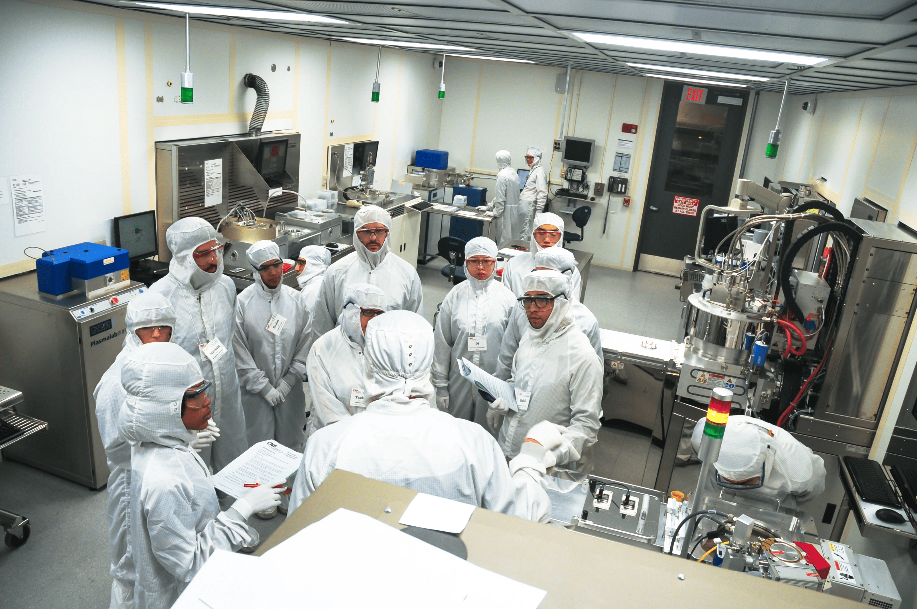
CNF serves as an open resource to scientists and engineers from a broad range of nanotechnology areas, with emphasis on providing complex start-to-finish tools centered on the nanofabrication needs of the research community. The research goals of our users are met at CNF by operating an expertly-staffed user program that provides, affordable, hands-on 24/7 open access to an integrated set of advanced nanofabrication tools.
The CNF offers a flexible, uniquely sophisticated toolset with over 180 nanofabrication and characterization instruments together with a track record of enabling successful research projects. Our user program has both regional and national scope, drawing researchers from throughout the US especially for projects that require particularly challenging multi-step micro- and nanofabrication processes, or access to unique instruments.
CNF continues to be an interdisciplinary facility with activities spread across the physical sciences, engineering, and life sciences. CNF actively seeks to stay at the technology forefront and is responsive to new user requests and research trends.
Every day we play a vital role in the intellectual convergence of many of the emerging engineering and science fields, bringing together researchers who provide clarity and vision to these fields and inspire young and diverse populations of students to pursue STEM studies.
What is the scope of the effort?
CNF, with its 17,000 ft2 cleanroom, 180+ tools, and the most advanced lithography equipment in network, serves on average 557 unique researchers/year from industry, government and academic institutions around the world. The average user from outside New York travels 950 miles.
CNF is arguably the oldest micro/nanofabrication user facility in the country, operating continuously and exclusively as a user facility since 1977.
CNF employs technical management, administrative staff, and a laboratory technical staff who maintain the equipment and baseline processes while assisting users at all levels – particularly focusing on the needs of our user community.
Support is provided by the National Science Foundation (NSF) as well as the NYSTAR/ESD Matching Grant Program from New York State.
What kinds of research does CNF enable?
As a user facility, ultimately the activities in CNF are dictated by our users, who believe we are the best place to realize their research goals. It is necessary to plan our activities to align with those areas that best align with significant future research directions, both within the Cornell faculty and elsewhere. Five focused areas have been identified that help guide our future research and efforts. These include Heterointegration, 2-D materials, Biotechnology, Quantum Materials and Devices and 3D Fabrication and Characterization. We believe these are the areas were CNF can have the most impact.
Heterointegration
The need for connecting and packaging wafers, chips, stacks of chips, electronics and photonics, and other heterogeneous materials has current needs among users and is growing. These can be complicated backend processes that may require highly customized methods include waveguide type interconnects as well as high pinout count packages. We envision increased applications of chips on chips, chips on flexible substrates, electronics on microfluidics, electronics on micromechanical systems, integration of photonics and electronics.
Device Research on 2-D materials
2-D materials, including graphene and TMDs (Transition metal dichalcogenides), have become increasingly important technologically, and increasingly of interest to CNF researchers. Cornell is also rapidly becoming a national center of activities in 2D materials. Thin film 2D materials are enabling both electronic structures with dramatic new electron, photon, and polariton properties and micromechanical structures based on graphene.
Increased Complexity in Biotechnology
For most of its 40 years, CNF has been a pioneer in the application of nanotechnology to the life sciences. Major activities include a variety of sensors and microfluidic devices. A new initiative in digital agriculture and the maturation of µfluidic chip technology make ripe the timing for more sophisticated tools and toolkits for biologists to engage in engineering projects to advance their research.
Materials and Processes for Quantum Devices
Fabricating and understanding a broad array of new materials provide the basis for advances in quantum information systems supporting a national imperative. CNF provides nanofabrication support to the new quantum materials and devices being designed and investigated nationally.
3D Fabrication and Characterization
Traditionally, micro- and nanofabrication have focused on thin film structures. New capabilities for 3D fabrication and characterization needed to meet the demand of the electronics, photonics, and life sciences communities are now available to users through our partnership with the Rapid Prototyping Lab in the Mechanical Engineering Department and the Cornell Institute of Biotechnology (Biotech).
Highlights of CNF-enabled research include:
- Origami-like 2D self-actuating microdevices
- Nano-optical structures for rapidly sequencing the genome
- Microfluidics that reveal information about cancer cell migration
- Distributed sensors for digital agriculture
- New meta-material flat optics focused with artificial muscles
- Quantum-entangled devices to usher in a new age of computing
- New nanosystems for more efficient energy creation
In each case, access to our tools, methods, and expertise has been critical to realizing a distinct research vision.
How do plasma processes such as dry etch and deposition contribute to your research?
Plasma etching is essential to the successful fabrication of many micro and nanoscale devices in electronics, photonics, MEMS, and quantum technology. Here at CNF, we have a plethora of etch systems, many of which are state-of-the-art, ICP-based, high-density plasma systems. That includes our latest Atomic Layer Etch system from Plasma-Therm. ALE produces highly anisotropic profiles with precise termination of the etch at a critical interface with little or no damage and preservation of surface stoichiometry.
Other benefits of ALE include etched wafer non-uniformities to less than 1%, along with pattern-independent based etching and high selectivity to an underlying layer. The ability to etch materials with resulting atomically smooth and flat surfaces can be extended to a wide variety of device applications in silicon, III-Vs, and 2D materials.
In the area of photonics, the fabrication of both passive and active optical devices is highly dependent on plasma etching to achieve perfectly anisotropic and smooth sidewalls for high quality low loss devices. We have been very successful in etching both dielectric and silicon-based waveguides, as well as active elements etched in both GaN and GaAs.
MEMS technology relies heavily on a few different etch strategies, one of the most important being deep reactive ion etching (DRIE). Here at CNF, we are fortunate to have 2 DRIE systems from Plasma-Therm. The time-multiplexed process allows us to fabricate devices in bulk silicon and bulk germanium. Those structures etched in Ge have been applied to the fabrication of x-ray optics used by Cornell’s High Energy Synchrotron Source (CHESS). CNF is also actively involved in piezo-MEMS research, which relies heavily on the etching of AlN and AlScN.
The fabrication of silicon, III-V and SiC based electronic devices requires an effective and highly specific etch strategy. This is especially appropriate in the fabrication of AlGaN/GaN HEMT enhancement mode lateral devices where the removal of AlGaN in the gate recess step is needed to carefully tune the threshold voltage. Care is needed to etch the AlGaN in a damage free manner so as to not degrade transistor mobility. These objectives are quite suitable for the application of ALE. For advanced silicon-based devices, the fabrication of through-silicon-vias (TSVs) is dependent on a customized high-quality deep silicon etches. In the area of silicon carbide devices, CNF has developed a smooth perfectly anisotropic SiC etch free of artifacts such as microtrenching, which are detrimental to device performance.
Plasma-based deposition systems are critical for the successful fabrication of devices in many technological areas. CNF has recently installed an HDPCVD system from Plasma-Therm. This ICP-based system will allow researchers to deposit films at low temperatures (80-150°C) for BEOL and thermal budget-limited devices. This system will also enable superior trench fill capability especially at high aspect ratios. This system is vital for fabricating electronic and photonic based devices. CNF is fortunate to have state of the art plasma enhanced atomic layer deposition (PEALD) for the formation of high quality thin high-k dielectric films. Films such as HfO2, Ta2O5, and TaN are essential in the development of advanced transistor devices.
A key addition for the successful development of piezo-MEMS devices is CNF’s OEM AlN deposition system. Plasma-Therm has recently acquired this technology from OEM. This dedicated AlN and AlScN system allows us to deposit high-quality, low-stress crystalline films.
Plasma etch and deposition technology are key wafer processing solutions for Quantum Information Processing and Quantum Sensing Devices. The formation of high-quality nitrides such as AlN and NbN via ALD are essential for high-performance Qubits and resonators. Effective etch processes are also needed for superconducting metals such as Al and Nb, along with Josephson Junction barrier layers such as Al2O3, AlN, and others. Smooth sidewalls free of residue with great profile control ensure surfaces of minimal loss. Quantum photonic components require ultra-smooth waveguide etches for low losses. TSVs enable 3D integration along with scaling to a larger number of Qubits. CNF has developed and continues to develop process solutions for these quantum-based process issues.