Today’s information age requires moving and manipulating vast amounts of data at the highest possible speeds with the lowest possible energy footprint. Photonics plays a critical role in achieving both goals. The photonics market is expanding rapidly, with the proliferation of cloud data centers and rapid growth of artificial intelligence (AI) driving the need for photonic integrated circuits (PIC).
Current inter-chip, chip-to-chip, and server-to-server interconnect technologies use copper, which causes latency and heat buildup in chips and servers. Heat impacts server performance, and due to the latency, additional servers are needed to achieve the desired results in a reasonable time. Copper interconnects also require more power to drive servers, and the resulting heat must be removed by cooling, which also drives up energy costs. Using optical interconnects between chips and servers has the potential to significantly improve processing speed and decrease energy consumption, creating a more sustainable computing environment. Intra-chip or on-chip optical interconnects are still in R&D and a few years away from introduction.
Other applications driving growth of the photonics market:
- Augmented reality (AR) headsets will be moving into the mainstream, driving photonics for consumer and enterprise virtual reality (VR) headsets for applications such as remote field service as well as the already-popular gaming applications
- Automotive markets are driving a large number of photonic applications on the path toward self-driving cars, including interior displays, exterior lighting, LiDAR used in lasers for automated driver assist systems (ADAS), and CMOS image sensors (CIS) used in cameras
- Laser diodes, called vertical-cavity surface-emitting lasers (VCSELS), are being implemented across a wide variety of applications, including telecom, medical, facial recognition, environment monitoring, infrared imaging, and even high-power lasers for industrial materials processing
- LiFi, an emerging photonics communications application, will potentially use lasers and LEDs for transmitting data at speeds about 100 times faster than can be achieved using WiFi
- Military, defense, and security applications for photonics range from imaging and mapping to enhanced communication and lasers
As these examples suggest, photonic semiconductors cover a wide range of territory, from solar cells to more sophisticated peripheral interface controller devices – MEMS, LEDs, CIS, digital signal processors, waveguides, and VCSELs. This creates a significant market opportunity for suppliers in this space.
Photonic Process Challenges
Manufacturing photonic devices presents unique challenges. Photonics wafer processing covers a wide array of wafer sizes and materials, such as mounting 100mm indium phosphide wafers to 300mm silicon wafers. With such a wide range of photonics devices, it is not unexpected that materials will be equally varied. Some of the common photonic materials are silicon (Si), silicon-on-insulator (SOI), silicon nitride, silicon oxide, gallium arsenide (GaAs), gallium nitride (GaN), indium phosphide (InP), and lithium niobate (LNO). As photonics technologies continue to develop, new materials will give photonic chips the ability to deliver greatly enhanced light-emitting performance for specific applications. It is easy to see that the materials and device requirements drive a range of process chemistries, hardware, and process control.
The process technology and equipment for photonics and their packaging cover a wide variety of unique materials and conditions. The Plasma-Therm team has a long history of process development for photonic devices that we have worked with our partners to commercialize. We’ve designed our unique set of process chambers to address the myriad processes required to bring photonic chips to market. The processing requirements for diverse devices include sloped profiles for microlenses and vertical profiles for waveguides in many different materials. Many of the processes are temperature sensitive and require conditions that range from cold to hot. These are just a few of the many requirements for processing wafers intended for photonics. The fabrication of a photonic chip typically involves a variety of process steps, and we have a product portfolio offering most of those process steps.
These chambers can be attached in any combination required for a customer’s unique process application – a key advantage of our approach. While most cluster tools for high-volume semiconductor manufacturing can implement only one type of process – for example, an etch or deposition chamber – for each position or facet on the cluster tool handler, we can provide any combination of etch, deposition, and clean to achieve the desired photonic process results. This is especially critical if the material is one that degrades when exposed to the atmosphere. We can configure a process sequence to etch, clean, and then deposit a passivation layer on the wafer surface, protecting the atmosphere-sensitive material.
The Versatility of VERSALINE®
Plasma-Therm offers the industry’s widest array of unique process chambers and solutions that can be placed on one system: our VERSALINE® platform. VERSALINE can perform a wide variety of processes, including inductively coupled plasma (ICP) technology, reactive ion etching (RIE), plasma-enhanced chemical vapor deposition (PECVD), high-density plasma chemical vapor deposition (HDPCVD), physical vapor deposition (PVD), ion beam etch (IBE), and high-density radical flux™ (HDRF) – versatility that comes in handy when you need to etch challenging photonic materials such as LNO. Selecting IBE or reactive IBE (RIBE) can improve the etch profile for LNO compared to ICP RIE technology, which may be the right option for etching a different material. Moreover, the multiple-chamber capability enables us to create multiple process flows for your photonic devices.
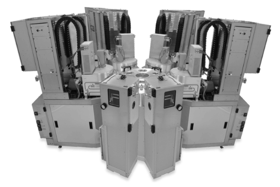
The VERSALINE platform’s flexibility enables us to configure the platform for R&D or high-volume photonics manufacturing using modules for wafers from 75mm to 200mm. We can also configure VERSALINE in multiple sequential configurations to provide the greatest level of flexibility for processing photonics. This allows us to offer a broader range of process solution options that can be found elsewhere in the marketplace. As an example, we can provide complementary processes on a cluster tool to avoid the atmospheric exposures traditionally needed. Sequential process modules that combine plasma etch resist stripping in a downstream system with passivation or metallization create a unique solution that avoids atmospheric interruption.
We match the VERSALINE process modules to our customers’ objectives and device requirements. For example, we provide critical technology that addresses devices with structures needing low damage and slow, controllable etch rates, or deposition systems with thin-film stress control, or those needing high-rate, high-aspect-ratio etching. Regardless of the specific process, it must include process control and manufacturability features. The systems support process control through EndpointWorks®, our endpoint detection system software platform. VERSALINE enhancements include data logging, an automated maintenance scheduler, and SECS/GEM communications. Our Cortex® control system provides a stable, user-friendly control interface designed for efficiency and productivity. Finally, our GLANCE software package allows extensive data collection and analysis capability for multiple chambers in manufacturing environments.
Plasma-Therm has nearly 50 years of experience providing unique processing solutions for photonic plasma etch and deposition on compound semiconductor materials. Let us put that experience to work for you. We offer the widest range of process technologies available for the photonics market, far surpassing competitors’ capabilities. Our VERSALINE platform’s modular design allows for a flexible configuration of both process chambers and substrates. Our substrate-handling options enable you to start at R&D using single-wafer configurations or carrier loading with a load lock and easily move to high-volume, multi-chambered production configurations as your process evolves. We also provide clear upgrade paths that leverage hardware and process development so you’ll experience lower cost-of-ownership and streamlined planning for your future photonic needs.