Tape Mounting After Partial Dicing
PDBG is done by partially etching the streets while the wafer is at full thickness. Once the streets have been etched to the desired depth, the wafer is then mounted to grinding tape. Upon grinding, the dies are separated when the grinding depth reveals the etched streets. The advantage of this approach is that any frontside processes can be done without the wafer being mounted to dicing tape or a temporary carrier. As with other plasma dicing approaches, PDBG offers the benefits of high wafer area utilization and stronger die.
Tape Frames
PDBG does not use tape frames for the plasma etching step, allowing conventional wafer-handling approaches.
Wafer Level Processing
With wafer on carrier, other processes such as lithography or metallization can be done without tape frames.
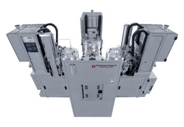
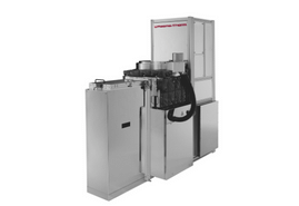
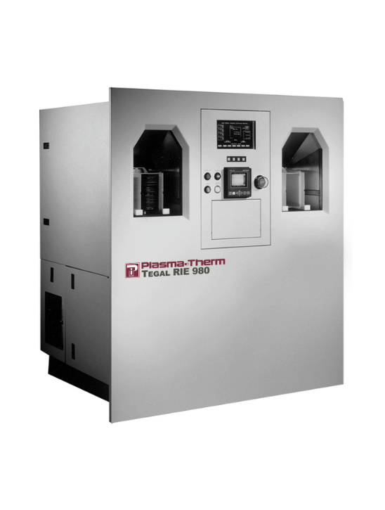
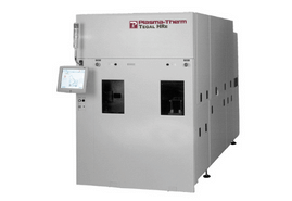
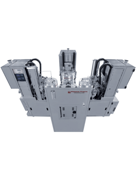
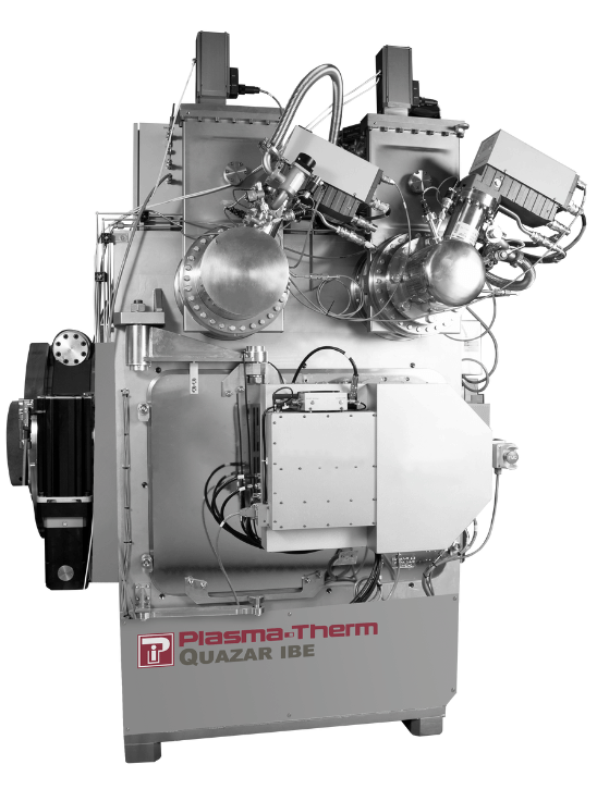
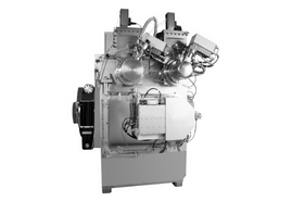
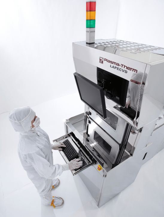
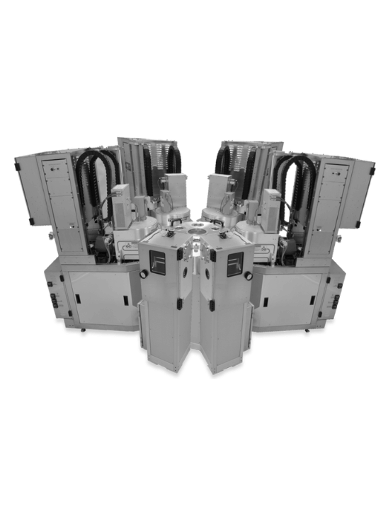
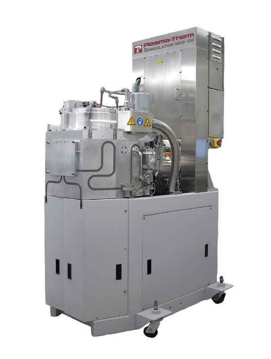
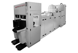
OUR PDBG PRODUCTS
EXPLORE TECHNICAL PAPERS
Want to learn more about this topic? Click here to review technical papers on PDOT principles, practices and outcomes.
SEE ALL SINGULATION PRODUCTS
To review all our singulation products, processes, capabilities, and brands, click here.
NEED ASSISTANCE?
Let our experts help you customize our processes solutions for your applications.