Archives: Process

PVD

Content

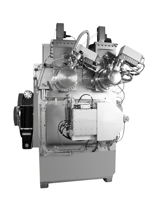
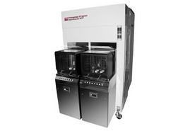
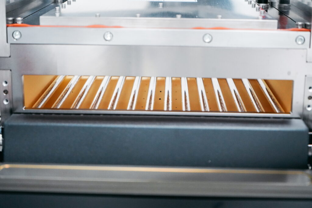
Physical vapor deposition (PVD) sputtering provides a reliable, reproducible, clean thin-film deposition approach. Using plasma and the appropriate targets, it creates films that are used for diverse applications. These include contacts and interconnects for frontside and backside metallization, piezoelectric films such as aluminum nitride (AlN) for RF filters, and films for quantum computing.

While the plasma in PVD is like  the plasma used for etching, in magnetron PVD systems ions are directed toward a target instead of the substrate. In response, the target ejects material that is destined for the substrate. Film properties are controlled with plasma power, target and substrate bias, pressure, and substrate temperature. The capability to add reactive gases gives the technology another dimension. 
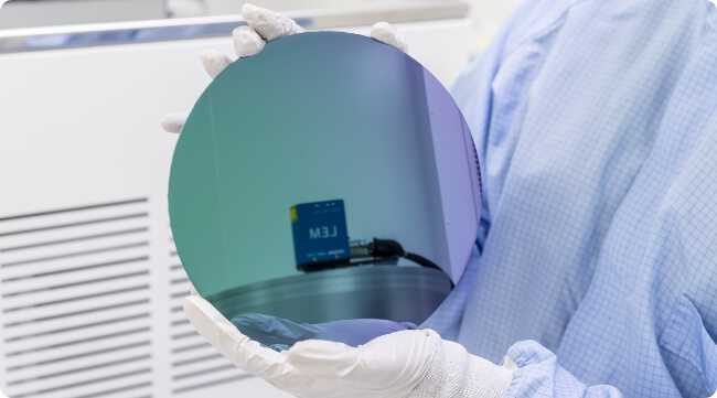
Specialty Films

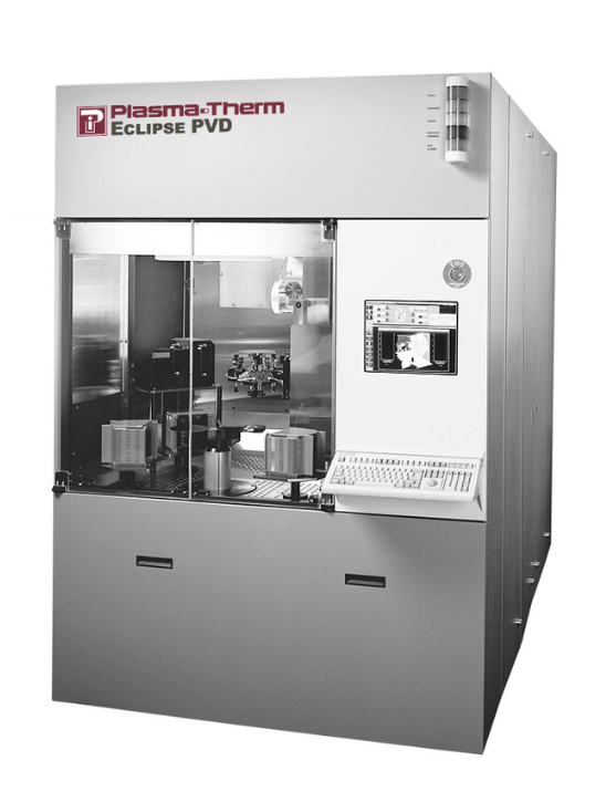
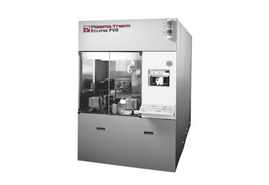
Plasma-Therm’s® products, Endeavor™ and Eclipse™, can also be used to deposit specialty films, such as aluminum nitride (AlN) and scandium-doped aluminum nitride (ScAlN), which need to be dense and oriented in a certain crystallographic structure. Other films, such as titanium oxide (TiO2), tantalum oxide (Ta2O5), and vanadium oxide (V2O5), can also be made using reactive mode sputtering. 
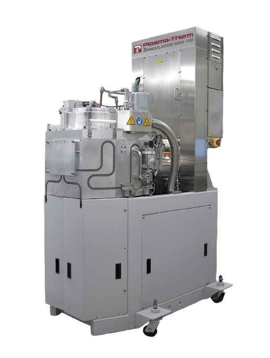
Sputtering Source

Both traditional magnetron and the proprietary dual-cathode S-Gun™ magnetron sources provide solutions as well.

OUR PVD PRODUCTS

EXPLORE TECHNICAL PAPERS

Want to learn more about this topic? Click here to review technical papers on PVD principles, practices and outcomes.

SEE ALL DEPOSITION PRODUCTS

To review all our deposition products, processes, capabilities, and brands, click here

NEED ASSISTANCE?

Let our experts help you customize our processes solutions for your applications.

IBD

Content

Ion beam deposition (IBD) provides control and repeatability for depositing a broad range of materials from dielectrics to metals, and everything in between. With such capability, the applications are extensive and include films for optics (antireflection coatings, filters, mirrors) and critical films for nonvolatile memory devices (MRAM) and magnetic transducers (thin-film read/write heads). With multiple targets, a complex film stack with angstrom-scale thick layers is possible.

The heart of the system is like ion beam etching: a plasma-driven ion source (usually driven inductively) with the Ar ions extracted and accelerated through a series of biased grids that can gently focus the beam. In IBD, the ions physically sputter material from a target to deposit it on the substrate. As with IBE, the substrate can be tilted and rotated for added flexibility. Ion-assisted deposition, where a second ion beam source is directed at the substrate where the film is being deposited, is a valuable optional capability. This makes it possible to influence film properties and even pattern structures using the tilt and rotate parameters. This multitude of features makes IBD a power approach to thin-film deposition.

Beam Targeting

In an IBD system, a biased grid assembly focuses a broad-beam ion source on a target. The ion beam strikes the target, causing the target material to be sputtered and then deposited on the substrate. 

Multiple Materials

A multi-target turret allows for the deposition of multiple materials without moving the substrate out of the vacuum environment. Advanced shielding avoids cross contamination. 

Multiple Parameters

IBD allows for control of multiple parameters, including ion energy, flux, species, and angle of incidence.

Independent Controls

Nearly independent control of these parameters is possible, which is a significant advantage for IBD over other sputtering methods.

OUR IBD PRODUCTS

EXPLORE TECHNICAL PAPERS

Want to learn more about this topic? Click here to review technical papers on IBD principles, practices and outcomes.

SEE ALL DEPOSITION PRODUCTS

To review all our deposition products, processes, capabilities, and brands, click here.

NEED ASSISTANCE?

Let our experts help you customize our processes solutions for your applications.

F.A.S.T.®

Content

At the intersection of ALD and CVD deposition methodologies, F.A.S.T. represents a cross between the two. Using liquid precursor vaporizers, a dual-channel gas delivery showerhead, and a capacitively coupled plasma generation configuration, films can be deposited with characteristics of both ALD and CVD. This produces conformal, ALD-like films at speeds more closely aligned to CVD. While it’s not for every application, F.A.S.T. is particularly suited for thicker films that ALD struggles with due to ALD’s slow deposition rate and films that do not require ALD’s level of conformality. With F.A.S.T. you get unique film properties, a best-in-class solution for thick and conformal layers, and ALD film performances at near-CVD speed. The result is a system with low cost of ownership.

Control

F.A.S.T. delivers temporal control for better film properties and separate species inlets with no parasitic reactions. Plasma pulsing adds another dimension to the flexibility offered by F.A.S.T. Liquid precursor vaporization provides precise volume introduction and repeatability. 

High Rate

In situ plasma with controlled overlap between precursor and reactant gases generates high deposition.

Cleaning

Chamber cleaning is facilitated with in situ capacitively coupled plasma. 

Applications

Examples include silicon oxide (SiO2) liners for through-silicon via (TSV) technology for 2.5D and 3D packaging and titanium nitride (TiN) for superconducting interconnects for quantum computing. 

OUR F.A.S.T. PRODUCTS

EXPLORE TECHNICAL PAPERS

Want to learn more about this topic? Click here to review technical papers on F.A.S.T. principles, practices and outcomes.

SEE ALL ETCH PRODUCTS

To review all our deposition products, processes, capabilities, and brands, click here.

NEED ASSISTANCE?

Let our experts help you customize our processes solutions for your applications.

HDRF™

Content

Some like it hot, some like it not. With Plasma-Therm®, you can have it both ways.

Our HDRF low temperature technology is proven for demanding applications. Remove photoresist and polymer residue without damaging your sensitive devices and complex structures – for optimal quality of Bosch-process devices.

Proprietary Source

HDRF technology incorporates a proprietary, distributed inductively coupled plasma (ICP) source

Source Design

The unique source design produces 50 to 100 times more radicals than other technologies and delivers damage-free process results

Before and After

The HDRF application portfolio includes scallop smoothing after DRIE, and surface activation before wafer bonding

Other Processes

Our high temperature stripping can also support descum and polyimide processes, as well as BCB, SU8 and PBO ashing

OUR HDRF PRODUCTS

EXPLORE TECHNICAL PAPERS

Want to learn more about this topic? Click here to review technical papers on HDRF etch principles, practices and outcomes.

SEE ALL ETCH PRODUCTS

To review all our material modification products, processes, capabilities, and brands, click here.

NEED ASSISTANCE?

Let our experts help you customize our processes solutions for your applications.

RTP

Content

Rapid thermal processing (RTP) was originally developed for ion implantation and annealing. It has since been expanded to include oxidation, silicide formation, chemical vapor deposition (CVD), and other advanced applications. Important characteristics of an RTP system include having a wide range of heating rates with a high upper limit, careful temperature monitoring, and ambient environment control. These capabilities make sophisticated thermal processing possible. 

RTP is a widely used technique with applications beyond silicon, including gallium arsenide (GaAs), silicon carbide (SiC), and other substrate materials. 

Temperature Control

With RTP, wafers can be heated from room temperature with rates as low as 40C/s to higher than 200C/s and can be held at a closed-loop controlled temperature before being ramped down. Pyrometer and thermocouple sensing ensure the necessary temperature control.

Multiple Processes

RTP can be used in a multitude of semiconductor process steps such as post-implant annealing, oxide and nitride film growth, reflow, and the formation of silicides, salicides, and metal alloys.

Temperature Uniformity

With the appropriate arrangement and control of the halogen lamps both above and below the substrate, the substrate temperature can be kept uniform.

Environmental Control 

By using a nitrogen curtain, unwanted oxygen (O2) can be kept to a minimum and monitored with an O2 analyzer. This same analyzer can be used to control the O2 concentration during oxidation processes. 

OUR RTP PRODUCTS

EXPLORE TECHNICAL PAPERS

Want to learn more about this topic? Click here to review technical papers on RTP principles, practices and outcomes.

VIEW ALL THERMAL PROCESSING PRODUCTS

To review all our material modification products, processes, capabilities, and brands, click here.

NEED ASSISTANCE?

Let our experts help you customize our processes solutions for your applications.

PDOT™

Content

On-tape, plasma-based die singulation is a fascinating way to approach die separation. It allows complete dicing of wafers of any thickness, especially thin and ultra-thin, on industry-standard tape frames after grinding. Plasma dicing on tape (PDOT) helps eliminate the rough edges left by blades and requires a much thinner cutting pathway than either blades or lasers. The key to PDOT is process selectivity and control, wafer and tape temperature management, and maintaining tape integrity. With a PDOT singulation system, streets can be narrower to allow more dies per wafer; dies are stronger, with no microcracking; and entire wafers are diced at once. PDOT is insensitive to shrinking die dimensions and increasing number of streets. 

Tapes and Frames

Industry-standard dicing tapes and a choice of conventional plastic or metal tape frames are available for PDOT.

Wafer Size Flexibility

Using an 8-inch frame accommodates wafers and pieces up to 8 inches in diameter. 

After Grinding

With thin and ultra-thin wafers, plasma dicing is done from the front side of the wafers after backside grinding, maintaining the simple process flow used with saw dicing.

No New Steps

Tape and frame integrity after plasma dicing allows for direct use of a grip ring for tape expansion and pick-and-place operation, with no additional steps.

OUR PDOT PRODUCTS

EXPLORE TECHNICAL PAPERS

Want to learn more about this topic? Click here to review technical papers on PDOT principles, practices and outcomes.

SEE ALL SINGULATION PRODUCTS

To review all our singulation products, processes, capabilities, and brands, click here.

NEED ASSISTANCE?

Let our experts help you customize our processes solutions for your applications.

Etch

At Plasma-Therm®, all our etch systems are founded in plasma-processing. Our plasma etching processes are more precise, cost effective, cleaner, and safer than wet etching. While wet etch processes use chemical etchants to remove materials, plasma etching converts gasses to plasma to selectively remove material. Plasma etching is used for semiconductor wafer processing, as well as in MEMS and compound semiconductor manufacturing. Performed under vacuum and often automated, We offer systems that perform the following plasma-etch processes:

ICP

When our inductively coupled plasma (ICP) technology is added to our reactive ion etching (RIE) system, you get higher etch rates, greater process flexibility and reduced ion bombardment for maximum process efficiency.

RIE

Plasma RIE etching is both efficient and gives you directional etching capability for maximum flexibility. RIE accommodates a wide range of materials. 

DSE™ 

When a smooth surface, excellent selectivity and etch depths greater than 100 µm are your goal, than ICP-configured Deep Silicon Etching (DSE) is your process of choice. 

IBE

When etch rate is less important than exacting profile control, ion beam etch (IBE) delivers. It offers you high precision for applications that demand targeted profile control.

ALE

Atomic Layer Etching (ALE) technology lets you control material removal from a substrate layer-by-layer, where the etch thickness is on the order of magnitude of a monolayer.

HDRF

Our HDRF low temperature technology is proven for demanding applications. Remove photoresist and polymer residue without damaging your sensitive devices and complex structures – for optimal quality of Bosch-process devices.

EXPLORE ALL ETCH PRODUCTS

Find all our etch products, processes, capabilities, and brands here.

CONTACT A SALES SPECIALIST

Terms and Conditions(Required)

Etch Product by Process Capabilities

Not sure which of our etch process tools is right for your applications? Use the table as your guide. 


* indicates products with Add-on options ICP RIE DSE™ IBE HDRF™ ALE
* VERSALINE®
ICP


RIE


DSE™


IBE


HDRF™


ALE

Tegal™  
RIE

       
Mask Etcher®
ICP

         
Odyssey        
HDRF™

 
QuaZar™      
IBE


NEED ASSISTANCE?

Let our experts help you customize our processes solutions for your applications.

Deposition

Deposition processes are used throughout the semiconductor manufacturing process to create integrated circuits (ICs). Nearly every step in the device fabrication process uses a form of thin-film deposition. Thin films are used in passive roles as hard masks, antireflection coatings, passivation layers, and encapsulation, as well as in active device roles such as capacitors, inductors, contacts, and interconnects. Thin-film materials include dielectrics, metals, and polymers. Many of them involve a plasma deposition process to deliver the desired film properties within a defined thermal budget. At Plasma-Therm®, we’ve fine-tuned an assortment of plasma-enhanced deposition processes to help you achieve precisely the film features you need for optimal device performance.

From dielectric films to metallization, dopants to anti-reflectant coatings and encapsulation, plasma-based deposition processes deliver on performance, precision, flexibility, and process control. 

PECVD

Plasma-enhanced chemical vapor deposition (PECVD) lets you maintain relatively low wafer temperature while achieving and controlling desired film properties such as stoichiometry, refractive index, stress, and step coverage, and also maintaining highly uniform film deposition.

HDPCVD

High-density plasma chemical vapor deposition (HDPCVD) is a special form of PECVD that uses an inductively coupled plasma (ICP) source to give you a higher plasma density than a standard parallel-plate PECVD system. For this reason, high-quality films are produced at even lower temperatures than with conventional PECVD. 

F.A.S.T.®

Fast atomic sequential technology (F.A.S.T.) stands at the crossroads of chemical vapor deposition (CVD) and atomic layer deposition (ALD). The technology is a derivative of ALD, benefiting from the flexibility of a dual-channel showerhead and pulsed gas injection with adjustable in situ plasma pulsing. The result is films that take advantage of ALD-like conformality but at significantly higher deposition rates.   

IBD

Ion beam deposition (IBD) is used to deposit thin films from a wide range of materials for various production processes. Tilt, substrate rotation, and ion-beam assist features provide capabilities not found in other deposition technologies. 

PVD

Physical vapor deposition (PVD) with sputtering technology allows for deposition processes of a wide range of metals for front- and backside applications and reactive sputtering of materials such as AlN, ScAlN, and AlOx.

Explore all Deposition Products

Find all our deposition products, processes, capabilities, and brands here.

CONTACT A SALES SPECIALIST

Terms and Conditions(Required)

Deposition Product by Process Capabilities

Not sure which of our deposition process tools is right for your applications? Use this table as your guide. 


* indicates products with Add-on options PECVD HDPCVD F.A.S.T.® IBD PVD
* VERSALINE®
PECVD


HDPCVD

 
IBD

 
QuaZar™      
IBD

 
Eclipse™        
PVD

Endeavor™        
PVD

KOBUS™    
F.A.S.T.®


NEED ASSISTANCE?

Let our experts help you customize our processes solutions for your applications.

Thermal Processing

Thermal processing provides control of time, temperature, and environment in a variety of semiconductor applications. In heat treatment processes used in semiconductor device fabrication, it’s important to control the heating ramp-up rate, hold time, and cooling ramp-down rate. Being able to raise the substrate temperature rapidly and then control it enables dopant activation, thermal oxidation, metal reflow, ohmic contact formation, annealing of damage, and even chemical vapor deposition (CVD). The extremely fast heating rates are typically accomplished with lamps due to their fast response times. Temperatures significantly greater than 1000C are possible. Beyond the applications mentioned, thermal processing can also be used to densify films and change the interfaces between film layers or between a film and a substrate.

Rapid Thermal Anneal (RTA) Technology 

RTA is a subset of thermal processing in which the wafer temperature reaches a point that may repair damage from etching or ion implantation processes. At the same time, it may also activate dopants. 

VIEW ALL THERMAL PROCESSING PRODUCTS

CONTACT A SALES SPECIALIST

Terms and Conditions(Required)

NEED ASSISTANCE?

Let our experts help you customize our processes solutions for your applications.

Click to access the login or register cheese