What do microns, nanometers, and angstroms all have in common? They are common units of measurement in the semiconductor industry. Prior to the mid-1980s, the semiconductor roadmap and most of the measurements performed in semiconductor manufacturing used microns and angstroms. Linewidths and pitch were measured in microns, and thicknesses were measured in angstroms.
The era of nanotechnology started in the late 1950s when U.S. physicist Richard Feynman started discussing processes by which scientists would be able to move and control individual atoms and molecules. The talk, titled “There’s Plenty of Room at the Bottom,” laid the groundwork for industries to explore nanotechnology.
Move forward to the 1980s, when the scanning tunneling microscope (STM) was developed and fullerenes, otherwise known as Buckyballs, were discovered – nanotechnology was now a reality. In 1989, IBM researcher Don Eigler spelled out “IBM” with 35 xenon atoms using the STM. Another key tool for the study of atoms and molecules emerged in 1986 when Gerd Binig, Calvin Quate and Christoph Gerber invented the atomic force microscope, which was commercialized in 1989. These revolutionary tools enabled researchers to look at what was happening on the molecular and atomic scale and allowed scientists and engineers to understand what was taking place on the surface of semiconductors.
The term “nanotechnology” didn’t gain momentum in the semiconductor industry until the launch of the National Nanotechnology Initiative (NNI) in 1999. When the NNI was funded in 2001, the U.S. semiconductor industry was all in. This timing coincided with the move to the 90nm (1 nm = 10-9 meters) technology node, which went mainstream in 2003. At this point, the semiconductor industry was probably the most highly invested in nanotechnology due to both shrinking transistor dimensions and the large number of companies challenging each other at the processing leading edge.
What Is Nanotechnology?
Nanotechnology is defined as the study and implementation of solutions centered on sub-100 nm molecules and atoms. The nanometer scale, 10-9 meters, is a unit of measurement that the semiconductor industry has homed in on for measuring and communicating the next generation of technology nodes. It’s not the only unit of measurement used in the semiconductor industry but has become prevalent since the transition from microns to nanometers (nm) for the definition of linewidths.
- 1 meter = 1,000,000 microns, or 10-6
- 1 micron = 1000 nm
- 1nm = 10 angstroms (Å)
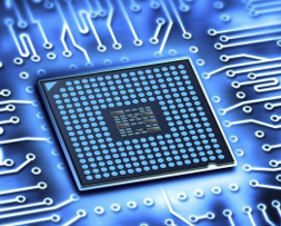
Over the past two decades, the semiconductor industry has transitioned from the 90nm technology node down to ever-smaller linewidths, achieving 3 nm in 2023. Technology nodes used to be defined by the metal half-pitch, but this is no longer the case. Today, they’re closer to what Drew Carey once said on Whose Line Is It Anyway? – “Everything is made up, and the points don’t matter.”
According to IMEC, at 3 nm the poly pitch is 44-48 nm and the metal pitch is 21-24 nm. These pitch dimensions produce chip features that are roughly 10-12 nm in size at the smallest dimensions. This is getting close to the atomic scale. Film thicknesses for the transistor gates at 3nm are in the 3-5 nm range, so a 3 nm silicon film is in the range of 15 atoms (with atoms being approximately 2 Å in diameter) thick. In the near future, two-dimensional materials are expected to be used in the semiconductor process. Materials such as molybdenum disulfide, tungsten disulfide, graphene, boron nitride, and others are being considered as the semiconductor industry seeks to continue extending Moore’s Law. These two-dimensional films are typically one atom or molecule in thickness. Nanotechnology is not exclusive to semiconductors; it is prevalent across the microelectronics space – nanometer films are processed in microLEDs (µLEDs) and optics – and in other industries as well.
Nanometer Processes
To achieve these nanometer dimensions, three primary equipment types are used in the electronics manufacturing process: lithography to define the features of the structure; etch to create the features on the structure; and deposition to deposit the nanometer film thicknesses on the substrate, creating the layers of the structure. Nanotechnology requires processes that are slow and controllable with little or no damage. Whether the feature is formed with etching or deposition, the rate must be relatively slow to achieve the requisite dimensions. The small scale means that any damage can be a significant fraction of the feature, and can have a significant impact on the yield. In many instances, we are etching or depositing just a few atomic layers, making uniformity critical for both processes.
In the microelectronics industry, several different pieces of process equipment are used for nanotechnology processing. For deposition, there is ion beam deposition, atomic layer deposition (ALD), plasma and thermal, and molecular organic chemical vapor deposition (MOCVD). In some cases, thermal CVD can also deposit nanolayers effectively. Depending upon the film thickness, deposition rates can be controlled by using surface rate-limited reaction techniques. In ALD, this is done by saturating the surface with one chemical, purging the chamber, and then introducing a second gas that completes the reaction.
For etch, atomic layer etching (ALE) is emerging for the removal of very thin layers. Similar to ALD, a reactive gas is deposited on the wafer surface in a monolayer. To complete the reaction, a second gas can be introduced, or a plasma can be pulsed. Conventional plasma etch is still used in a significant number of nanotechnology etch applications, but great care is taken to slow the etch rate to minimize the removal of key films; to use gas chemistry to help protect critical layers; or to use low bias or downstream etching techniques to limit ion bombardment on the critical surfaces.
Plasma-Therm Nanotechnology Expertise
At Plasma-Therm, we have significant expertise in nanotechnology processes. In the deposition space, we have products that use ion beam deposition to deposit uniform nanolayers for optics, MRAM semiconductors, and thin film heads. Nano-layering of complex film stacks is also possible. In the ALD segment, Plasma-Therm’s Fast Atomic Sequential Technology (F.A.S.T.®), or F.A.S.T. ALD, enables atomic layer films at higher deposition rates than conventional ALD processes. F.A.S.T. deposits conformal nanolayer films at CVD deposition rates, shortening cycle time and time to market.
On the etch side, Plasma-Therm’s ion beam etch (IBE) technology enables targeted profile control and exacting thickness precision for specific nanotechnology processing. This technology is used for MRAM, surface acoustic wave (SAW), and bulk acoustic waver (BAW) filter trimming. Our VERSALINE® platform offers the widest selection of nanotechnology etch options, starting with our ALE process. Below 10nm, precise control of etching layers is crucial. Our customers can precisely etch one layer at a time using our self-limited ALE technology.
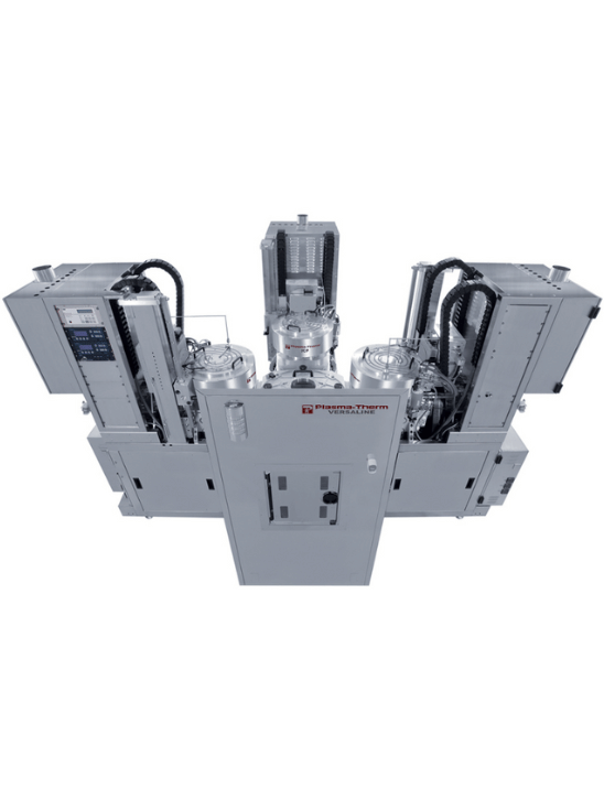
Our current ALE capabilities include silicon, silicon dioxide, silicon nitride, III-Vs material, 2D materials, and selected metals. VERSALINE also incorporates conventional etch technology that is used to create nanotechnology features. Our inductively coupled plasma (ICP) technology reduces ion bombardment, minimizing damage on the wafer surface. Our high-density radical flux (HDRF) chamber ensures damage-free removal of polymers and photoresist. These specific low-damage etches combine well with Versaline’s other etch processes, reactive ion etching (RIE) and deep silicon etch (DSE).
Together, Plasma-Therm’s offerings provide customers with an arsenal of tools that will enable them to solve any nanotechnology process challenge for today or tomorrow.